It is possible to make the Printed Circuit Boards (PCB) thinner using a femtosecond laser.
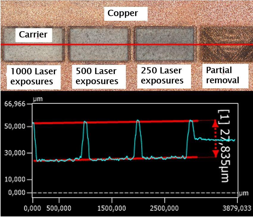
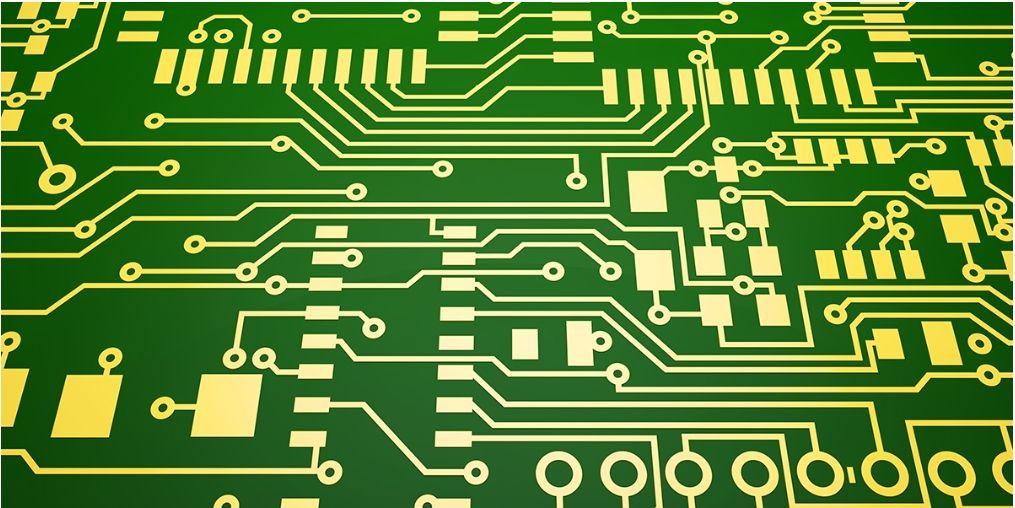
Printed Circuit Boards (PCB) are used for connecting electronic components such as ICs, transistors, resistors, etc., (see figure below). The base is made of an organic material covered with a layer of copper wherein electrical connections between the components are etched. Attempts are being made to make the layers increasingly thinner in order to achieve miniaturisation, functionality and savings on materials costs.
Using a femtosecond laser it was possible to write a pattern in a 20 micron copper layer while removing less than 10 micrometres of the base. Process tuning made it possible to increase the selectivity to the fibres and matrix of the organic base, avoiding further recess even with an increased number of laser exposures. This meant that copper residues could be selectively removed. Hence, femtosecond laser technology can be used for advanced PCB prototyping. It allows the definition of the electrical paths down to a level of 10 microns without the necessity of masks.
It is possible to make the Printed Circuit Boards (PCB) thinner using a femtosecond laser.
(Source: Nutvolts)